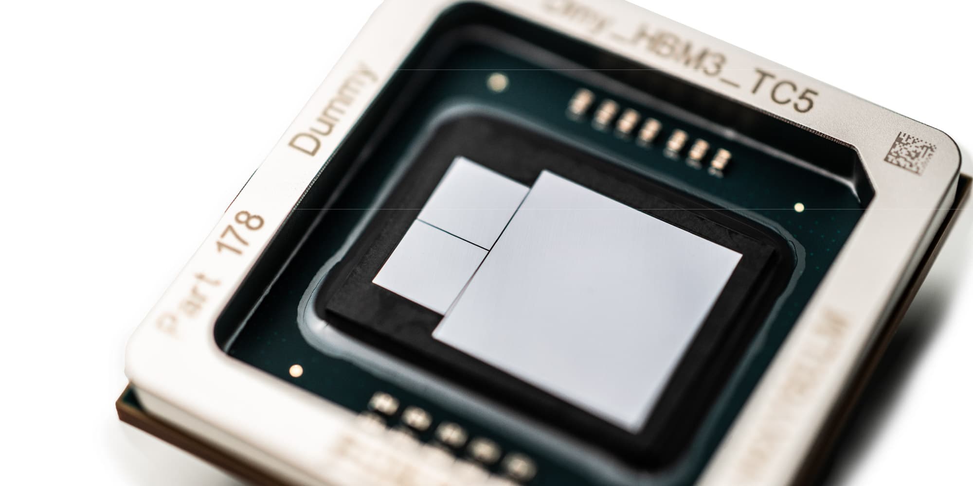
GaN-IC prototyping through multi-project wafer service (MPW)
Want to affordably produce a small volume of integrated GaN-IC power devices in a superior technology? Then reserve your space on a multi-project wafer shuttle.
Gallium nitride (GaN) offers a lot of benefits as a power conductor. But it only unleashes its full potential when incorporated in an integrated circuit (IC) that acts as a tight and high-performing power device.
The development of such an integrated power system is a complex matter. But it’s accessible – even in small volumes – thanks to IC-Link’s multi-project wafer service (MPW).
Share the costs of your GaN-IC fabrication
The principle of an MPW service is that you reduce some of the biggest costs of IC manufacturing – such as engineering, processing and masking – by splitting them with other customers.
You then get a limited amount of chips, for instance for a validation or launch of your product. Once you’re ready to grow, you can easily scale up to dedicated runs.
An improved way to make GaN-ICs
The big challenge when it comes to integrated on-chip GaN-IC power systems is the lateral isolation of the devices. This is needed to avoid parasitic inductance. IC-Link gives you access to imec’s GaN-on-SOI technology that allows trench isolation. It avoids the use of a shared Si substrate that can only be referenced to a single potential at a time.
The result is a monolithic integration that achieves high power density and huge switching speeds within a tiny device.
Ready to get started?
Technical details
Technology characteristics
We epitaxially grow a GaN layer on a 200mm SOI wafer (Si(100)/SiO2/Si(111)). We achieve this through metal-organic chemical vapor deposition (MOCVD). The stack contains several layers:
- AlN nucleation
- (Al)GaN buffer
- GaN channel
- AlGaN barrier
- Mg-doped p-GaN
We perform precise strain engineering to manage the stress that builds up in the wafer during growth. The result is a GaN-on-SOI wafer with regulated warpage and excellent mechanical strength. Moreover, we can process e-mode p-GaN HEMTs and use TiN/p-GaN stacks for the gates.
Highlights
- combination of multiple transistors on a single chip through trench isolation
- saving of costs by packaging one instead of many devices
- reduction of system parasitic inductance
In order to reach the highest switching speed of GaN power devices, the parasitic inductance should be reduced by co-integrating the drivers. More functionalities can be included by the low-voltage logic and analog switches, the high- and low-ohmic resistors and the integrated MIM-capacitors.
Application domain
High-power switching and power conversion: 100V and 650V.
Tools (front- and back-end)
Cadence
Verification tools
DRC Calibre
Library
The PDK contains process documentation, library devices, layout guidelines for custom design, verification and models.
- low- and high-ohmic resistors
- metal/oxide/metal capacitors
- metal/insulator/metal
- low-voltage logic devices
- Cu RDL special features
Usual turnaround time
After submission of the final DRC version, the process takes about twenty weeks. DRC iterations will happen during six weeks before the submission.
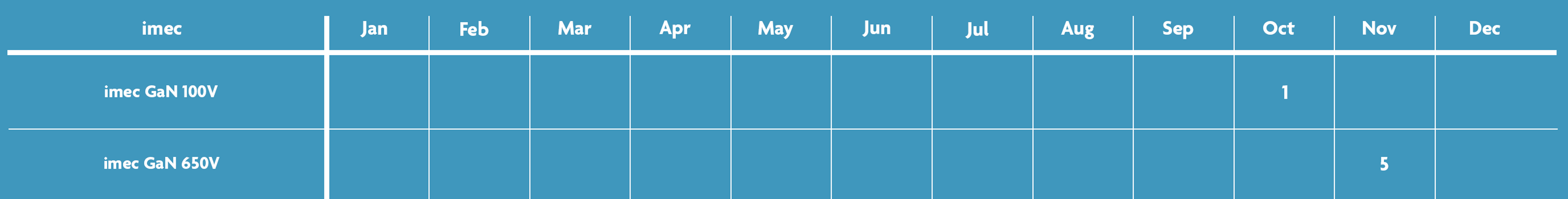
MPW schedules 2025
For imec GaN IC on SOI
Important notes:
- Dates indicate deadlines for submission of the first version of the GDS file.
- Registration for a given shuttle closes one month before the dates indicated on the table.
- The administrative procedure must be finished at least 1 week before the dates indicated on the table.
Standard MPW prices
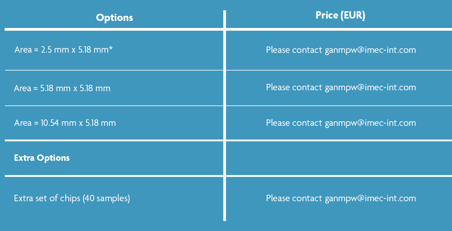
Important notes:
- Regular number of samples is 40.
- Due to the nature of MPW logistics, more chips than ordered may sometimes be shipped.
* This option is only available to academic institutions.
**Per additional dicing lane, following MPW templates only.
**Sub-dicing options must be approved by the technical team. Please contact ganmpw@imec-int.com in advance to evaluate your request.
Dedicated GaN-IC runs
Imec’s GaN-on-SOI and GaN-on-QST® technologies are available through dedicated runs.
- You get 12 full 8-inch wafers with your devices.
- We process the lot as soon as we receive the mask.
- The lead time is ~19 weeks if a DRC clear GDS is received.
For more information about the conditions and price, contact us directly at ganmpw@imec-int.com.